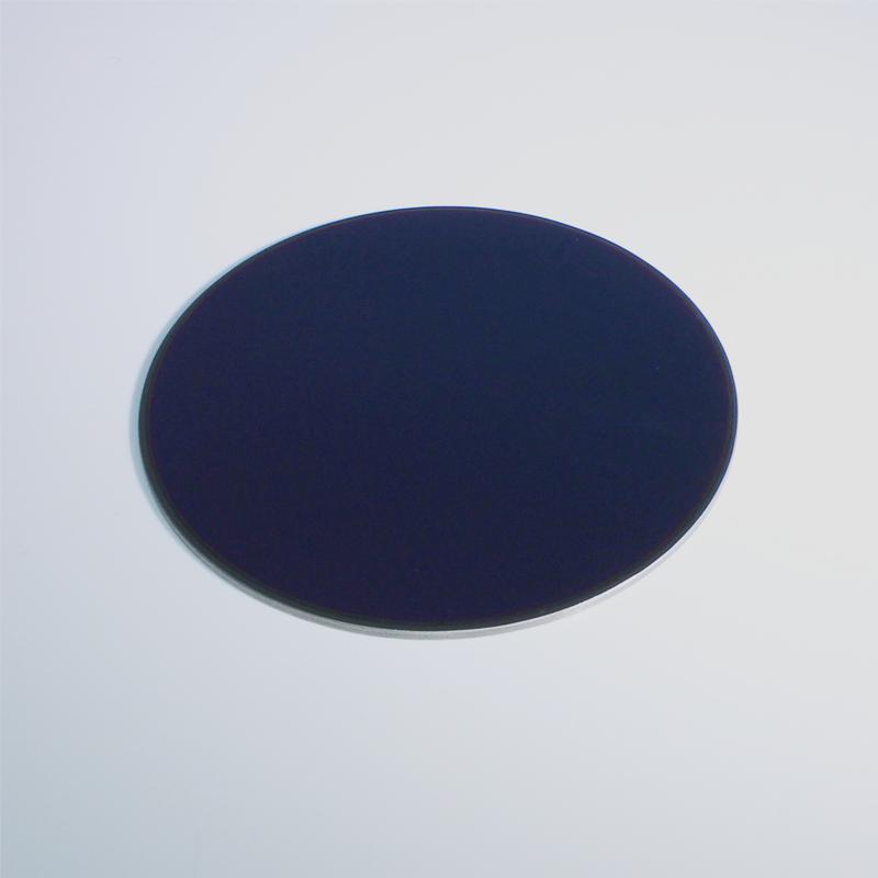
D55mm*T1mm Si (Silicon) Wafer with AR coating @7-14 um
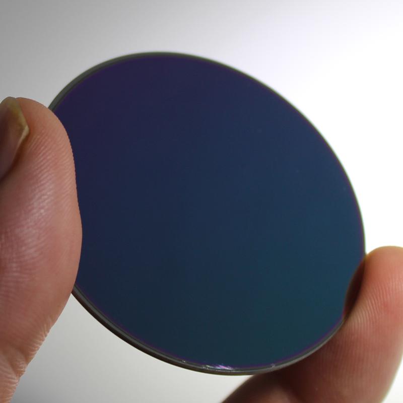

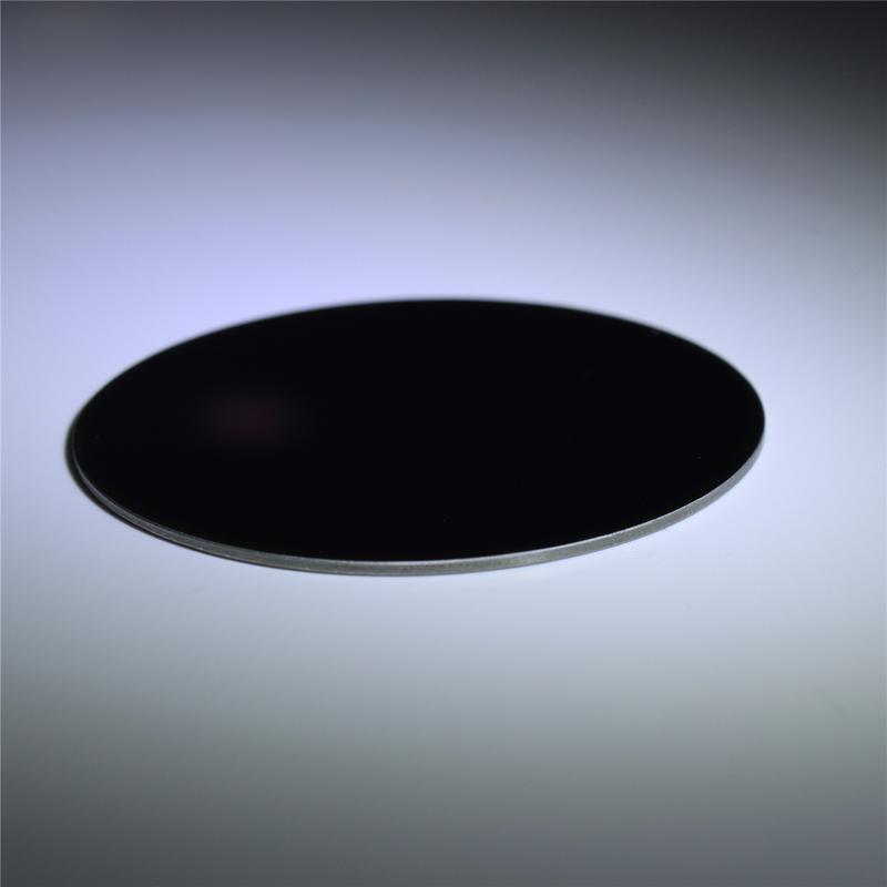
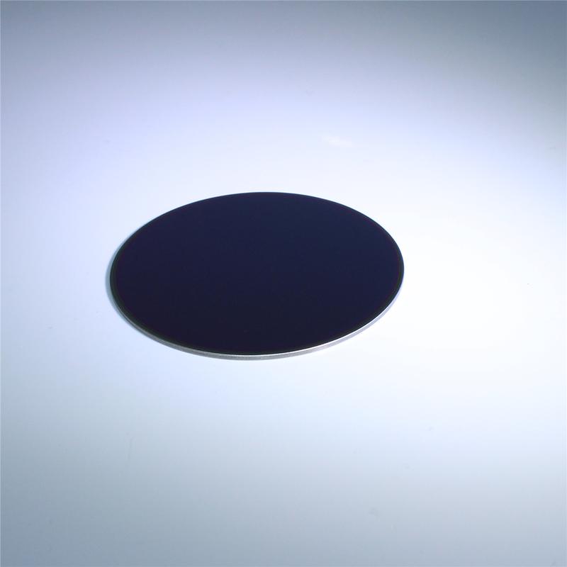
D55mm*T1mm Si (Silicon) Wafer with AR coating @7-14 um
Item Number:VY_20B2T64Si
- Material: Silicon
- Dimension: Dia.55mm
- Thickness: 1.00mm
- Tolerance : +/-0.10mm
Silicon wafers are a key component of integrated circuits such as those used to power computers, cellphones, and a wide variety of other devices. A silicon wafer (Si wafer) consists of a thin slice of silicon which can be treated in various ways, depending on the type of electronics it is being used in. Silicon is a very high quality semiconductor, making it ideal for the production of such circuits, although other materials have been explored historically.
Question one: What is a Silicon Wafer?
To begin we will explain silicon and the characteristics of this element that make it appropriate for our uses. Silicon is the second most common element on Earth and it is the seventh-most common element in the entire universe. It is the most common semi conductor and the most widely used in the electronic and technology sector. There are different silicon fabrication methods including the horizontal gradient freeze method, the horizontal bridgeman method, the vertical bridgeman method, the vertical gradient freeze and finally the Czochralski pulling method.
During the growth process intentional additions of dopants can be added to the to change the purity of the silicon depending on what the purpose of it will be. These introduced impurities can change the electrical properties of the silicon, which can be useful depending on what the silicon is ultimately being produced for. Boron, aluminum, nitrogen, gallium and indium are just some of the silicon dopants that can be introduced during the growth process. Depending on what level the silicon has been doped, the semiconductor can be considered extrinsic or degenerate. Extrinsic would be lightly to moderately doped whereas degenerate semiconductors act more as conductors because of the high levels of doping that occurs during the fabrication.
Question two: What is a Si Wafer used for?
As it was mentioned before, silicon wafer’s primary use is in integrated circuits. Integrated circuits power many of the devices that modern society uses everyday. Computers and smartphones are just two of the devices that are dependent on this technology. Although other semiconductors have been tested overtime, silicon has proved to be stable option. Other uses include sensors, such as the tire pressure sensor system, and solar cells. Silicon wafers absorb the photons in sunlight and this in turn create electricity.
Many companies use silicon wafers in their product testing. In this purpose, a lot of time the product or prototype is created and tested. Through this testing the silicon wafer can become damaged and although in the past this would lead to the wafer being discarded and a new wafer being purchased for further testing. With the technology Wafer World has created, however, companies are saving millions! Give us a call at 86-431-84631230 or contact VY Optoelectronics Co.,Ltd. online for all of your wafer needs! We are committed to producing quality wafer products, so contact us freely!
Related Products
Silicon Wafer Blank
Chinese ZnSe Lens
Germanium (Ge) Windows